


Lead Frames
Fast and economical manufacture of high lead/pin count, ultra-fine pitch lead frames.
Request Pricing Application NoteOur lead frame manufacturing service has the flexibility to meet the fast-paced nature of the electronics industry, and the precision required to manufacture ultra-fine pitch, high pin count lead frames more cost-effectively than stamping.
WHAT ARE LEAD FRAMES?
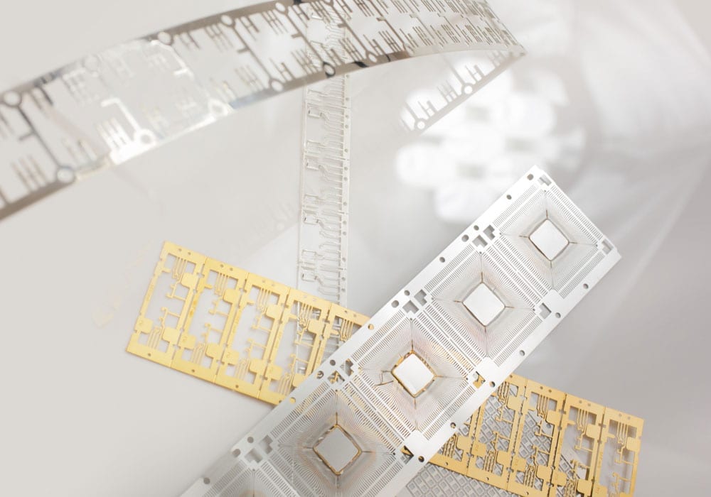
Lead frames play a crucial role in the assembly of semiconductor devices. Manufactured from a range of copper-based alloys, they serve as thin layers of metal, connecting the wiring from small electrical terminals on the semiconductors surface to the large-scale circuitry on electrical devices and circuit boards.
Traditional lead frame stamping
Lead frames are typically manufactured in high volume using stamping. However, this method has several drawbacks, including burrs and stresses that can negatively impact the performance and efficiency of the lead frame. Moreover, stamping complex designs and geometries, which are crucial when producing thinner or miniaturised lead frames, can be both time and cost prohibitive.


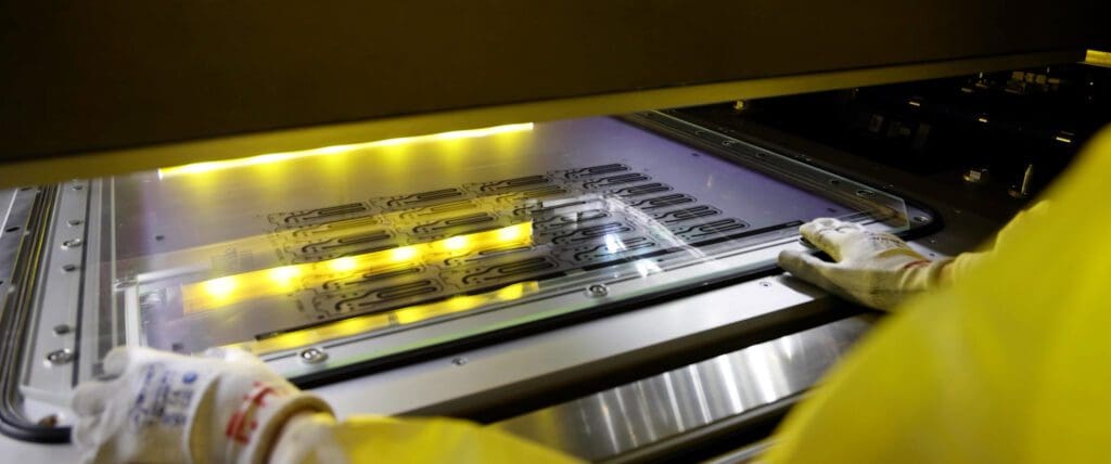
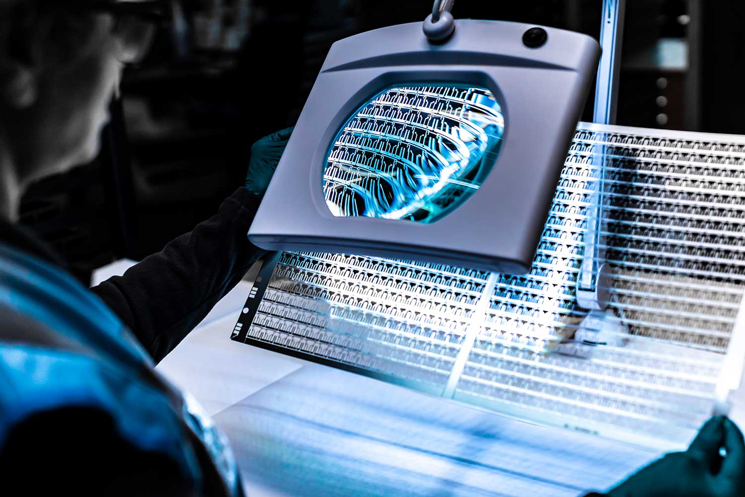
Photo etching lead frames
Our photochemical etching service provides high-quality lead frames free from defects – effectively overcoming the challenges encountered using stamping technology. We offer lead frames from copper or iron-nickel alloys, such as alloy 42, which demonstrate very low thermal expansion. Additionally, we provide a variety of post-process options, including forming and tin, silver and gold plating, improving wire bond attachment to the semiconductor die.
Benefits

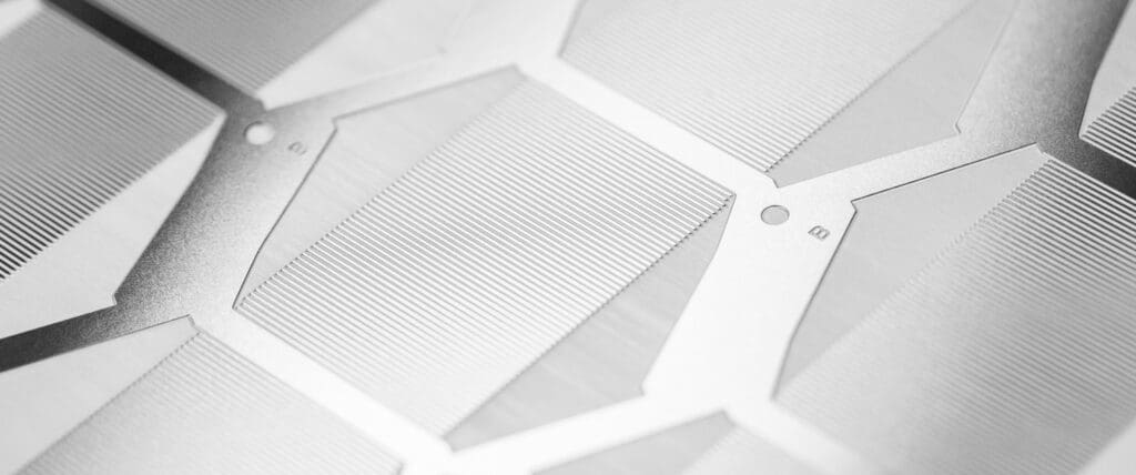
Flat, stress and burr-free

Rapid prototyping

Accuracy to ±0.020mm

Low cost tooling
Up to 90% faster than stamping
Photo etching uses digital tooling, removing the need to cut expensive and difficult to adapt steel moulds. Digital tooling also provides engineers with endless design possibilities without cost penalty.
Our production capabilities allow us to manufacture miniaturised features as small as 0.1mm and achieve accuracies of ±0.020mm. This makes it ideally suited to a range of ultra-fine pitch lead frames applications.
Lead Frames Application Note
Explore how etching can enable compact and intelligent packaging solutions for semiconductor lead frame designs.
DownloadRelated Articles
The economic manufacture of lead frames – a technical comparison
Precision Micro have created a technical comparison of the economic manufacture of lead frames.
Read More