

The economic manufacture of lead frames – a technical comparison
A lead frame is utilised in the semiconductor device assembly process and is essentially a thin layer of metal that connects the wiring from tiny electrical terminals on the semiconductor surface to the large-scale circuitry on electrical devices and circuit boards.
Lead frames are used in almost all semiconductor packages. Most kinds of integrated circuit packaging are made by placing the silicon chip on a lead frame, then wire bonding the chip to the metal leads of that lead frame, and then covering the chip with plastic. This simple and usually low-cost packaging is still the best solution for many applications.
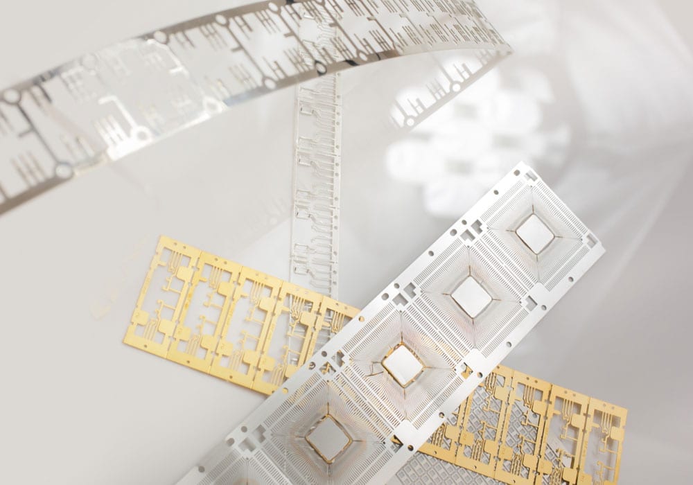
Typically, lead frames are produced in a long strip, which allows them to be quickly processed on assembly machines, and two manufacturing processes are normally used, chemical etching (often seen as most suitable for low to medium volume production), and stamping (most often associated with high volume production runs).
In lead frame design, one size does not always fit all, and very often demand is for customised specifications and features, designs that enhance electrical and thermal properties, and specific cycle time requirements. Precision Micro has in-depth experience of lead frame manufacture for an array of different customers using chemical etching, and this article details the nature of the company’s work in this field.
Different technologies for lead frame manufacture
Chemical etching
Chemical etching is one of the most popular and widely utilised methods for the manufacture of lead frames. While perhaps perceived as a high-unit-cost process, tooling is very low cost and extremely time-efficient.
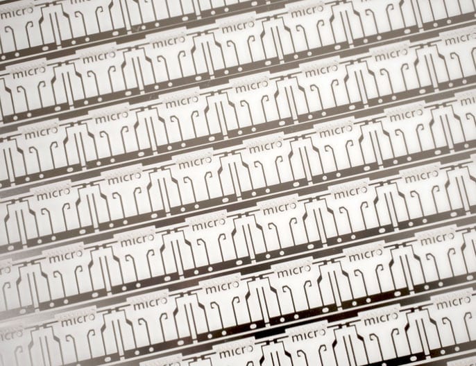
Etched lead frames are manufactured in flat sheets usually made out of either copper or iron-nickel alloys (such as alloy 42) that demonstrate a very low expansion rate at room temperature.
These low thermal expansion alloys have found use in modern applications which require joining of a metal to glass or ceramics and in areas that demand the same thermal expansion rates for materials to be joined in order to prevent associated problems within the joint area.
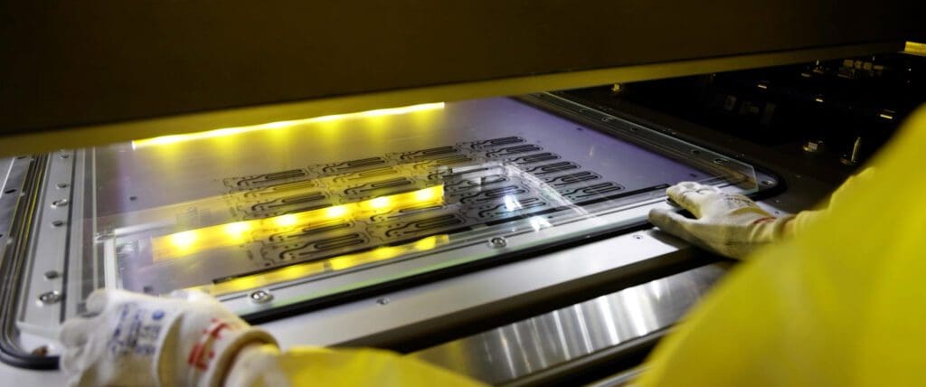
Both sides of the flat alloy sheets are cleaned and then laminated with photo-resist. The photo-resist is then exposed to the required lead frame pattern with the aid of an ultraviolet source and a precision pattern film. The resist is developed over the areas that are to be etched away, with the remaining resist protecting the parts during the etching process.
Finally, the protective photo-resist is stripped from the finished lead frames, before the etched panels are singulated into strips, or supplied in sheet for easy handling depending upon customer requirements. The cut strips are cleaned and plated, usually with silver at the inner leads to facilitate wire bonding. The plated strips are then ready for final inspection.
Stamping
Stamping is an automated, high-speed process suitable for large production rates that make the initial high tooling costs tolerable. The sheet metal – typically in roll form – is pierced along both edges to create indexing holes that position the sheet during further processing. The location holes are used to advance the sheet metal strip through the stamping machine. Die-and-punch sets specific to the lead frame geometry are also required.
The process is typically accomplished by a series of stamping operations that progressively approach the final lead frame geometry, the number of steps being entirely dependent on the complexity of the geometry of the lead frame.
What is the right method for you?
Lead frame production volume is a key consideration in manufacturing process choice, with stamping in general terms being most economical for very high production volumes, and chemical etching for low to medium scale production runs.
This is almost entirely a product of the respective tooling costs.
The tooling for chemical etching is digital, so there is no need to start cutting expensive and difficult to adapt steel moulds. This means that large quantities of lead frames can be reproduced with absolutely zero tool wear, ensuring that the 1st and the 500,000th part are exactly the same.
Also, as the tooling is “virtual”, it can be adapted and changed extremely quickly and cheaply, making it ideally suited for anything from prototype runs to high volume production runs. This allows for design optimisation without financial penalty, and helps ensure a low-risk entry strategy as well as facilitating easy product updating. Turnaround time using photo-tools is about 90% less than that for stamped frames. Stamping requires substantial investment in mould fabrication which is not only costly but in some instances can take from six to ten months to complete, compared with a few hours for etching.
But beyond the tooling time and cost differences between the two processes, there are other inherent aspects of the chemical etching process that require all lead frame manufacturers – be they manufacturers of low, medium, or large volume runs – to sit up and take notice.
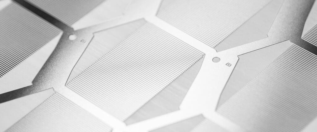
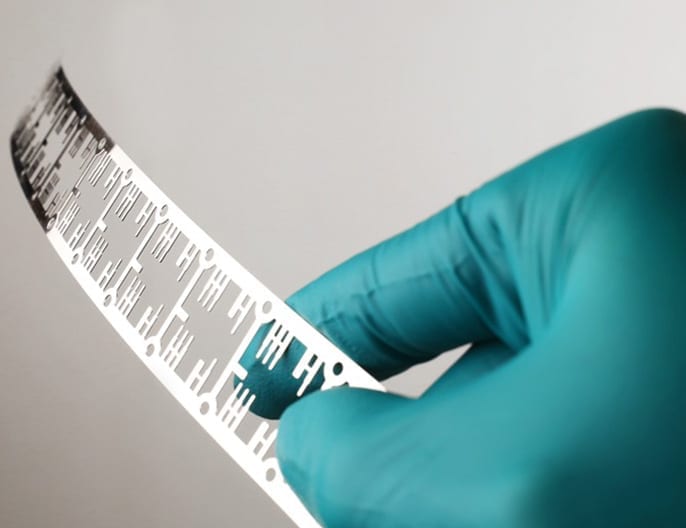
Lead frames can often be extremely complex and also very fragile. Indeed, in many instances, geometric complexity and the requirement for extremely exacting tolerances and precision mean that chemical etching is not just a potentially desirable manufacturing process but is, in fact, the only technology able to make certain lead frames.
Let’s take a closer look at the complexity conundrum
When stamping lead frames, complexity adds cost, whether in low, medium, or high volume applications. The complexity of the lead frame means the necessity for a complex mould tool, and complex tooling means increased costs, increased potential for tool failure, and increased lead-times for satisfactory completion.
With chemical etching, it makes no difference in terms of costs or lead-time how complex the geometry of the part is as the component image is printed directly onto the metal sheet in a single process.
Also, chemical etching can also produce lead frames with tighter tolerances and finer detail than is possible with stamping, and all with minimal if any degradation and deformation of the metal being processed, and little to no likelihood of burrs or defects. Failure rates are minute, and unlike in the stamping process, every lead frame produced is absolutely flat.
However, of course, stamping does have its place. Whereas chemical etching’s “sweet spot” is in the manufacture of complex lead frames in small to medium sized production runs, in extremely high volume runs where the tooling expense is justifiable, and where designs are not overly complex, stamping typically represents a more economical process.
In essence, the stamping process is simple. It fabricates a lead frame by pressing a substrate into a mould, and forming a certain shape while sequentially transferring the substrate using a sequential transfer press moulding device. Chemical etching is an altogether more complicated process, hence its ability to be applied to complex geometries and to achieve exacting levels of precision. The increased number of variables in the process can increase the possible margin of error, but this can be mitigated if partnering with a company expert in the chemical etching process such as Precision Micro.
In addition, etching cannot be used on pre-plated strip. Here, stamping is often the required option, as etching through the plating can lead to etch differentiation and inaccuracies. For etching to be used with plated strip, the process would need to etch first, and then plate after etching, making a one step process a two-step process, and therefore adding to costs. However, there are instances where the volume of run or the complexity of lead frame makes even this two-step “etch and plate” process desirable.
Stamping also forms the lead frame pins at the same time that the parts are stamped out of the strip, and again, with chemical etching, this is a two-stage process with a possible knock-on effect on cost efficiency.
Precision Micro and lead frame manufacture
So far, this article has looked at the general considerations when choosing between stamping and chemical etching in lead frame manufacture. But there is one more variable that needs to be added into the mix, and that is the expertise and experience of your chosen manufacturing partner.
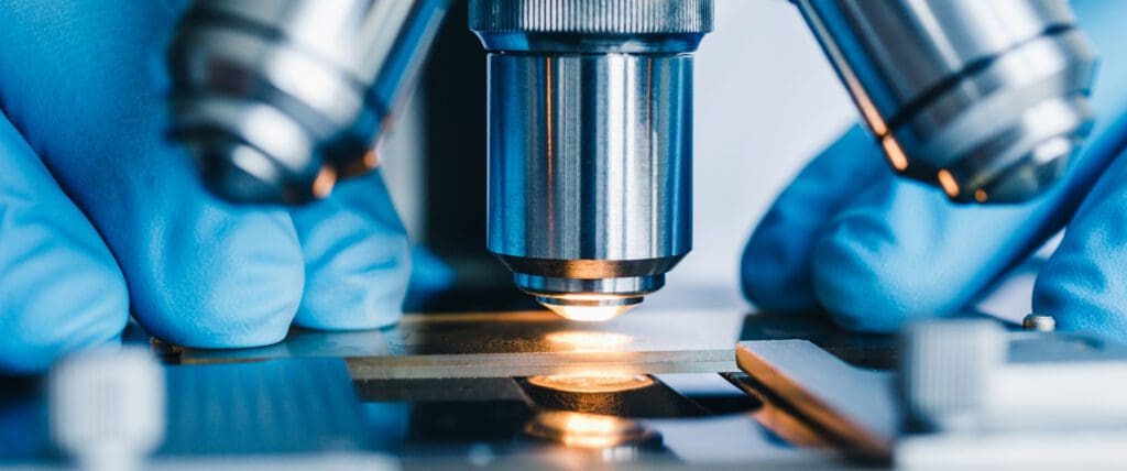
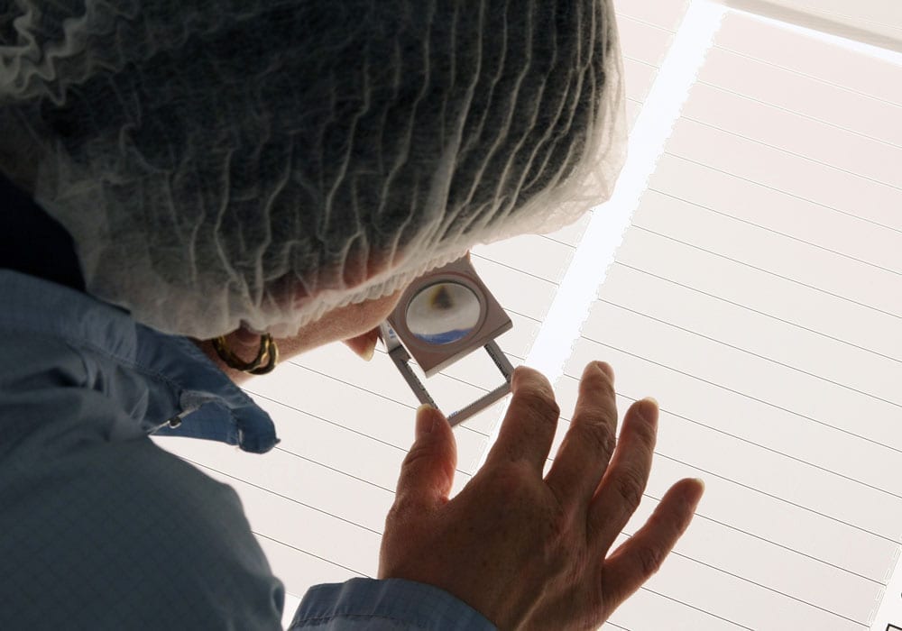
Take, for example, the potential for increased margin for error due to the number of variables in the chemical etching process. Leading European chemical etching specialist Precision Micro has a robust, repeatable method of lead frame manufacturing due to years of experience in this area, which cannot necessarily be matched by other chemical etching service providers. To a great extent, this experience which stretches back over 5 decades mitigates areas where chemical etching may generally be regarded to have weaknesses. The company has invested heavily in process control to reduce variation, as well as optical inspection to achieve zero parts per million failure rates.
Precision Micro has unmatched experience in the production of bespoke lead frames, in conjunction with some of the world’s leading semiconductor packaging companies. The company’s tight tolerance manufacturing processes are appropriate for numerous lead frame applications but are ideally suited to high lead/pin count, ultra fine pitch lead frame manufacture.
Conclusion
In very general terms, to say that stamping is best suited to high volume manufacture of simple lead frames, and photochemical etching is best suited to low-medium volume manufacture of complex lead frames is accurate.
However, Precision Micro is continually evolving and developing the photochemical etching process, and as such its applicability to a diverse number of applications is growing every day. The company is able to challenge industry preconceptions about the use of photochemical etching, and the area of lead frame manufacture exemplifies this perfectly.
With the inherent advantages of the process in terms of its ability to manufacture extremely complex parts to high tolerances, and the easy adaptability and cost-effectiveness of the associated tooling being a given, Precision Micro’s expertise adds more and more possibilities for lead frame manufacturers.
Even the premise that stamping is the only economic process for high volume lead frame manufacture is being challenged as Precision Micro works continuously towards process automation.
Chemical Etching Whitepaper
Learn how chemical etching can overcome the limitations of traditional sheet metal machining technologies.
DownloadLatest Articles