
PCB shielding explained: An essential guide to effective PCB shielding
In our technology-driven era, the issue of Electromagnetic Interference (EMI) presents a continuous hurdle as we increasingly depend on electronic devices. As a result, the importance of implementing effective shielding techniques at board level is paramount.
In this article, we explore the importance of printed circuit board (PCB) shielding, how it is manufactured, and the benefits of using chemical etching or stamping to manufacture cost-effective shielding solutions which meet time to market demands.
What is PCB Shielding?
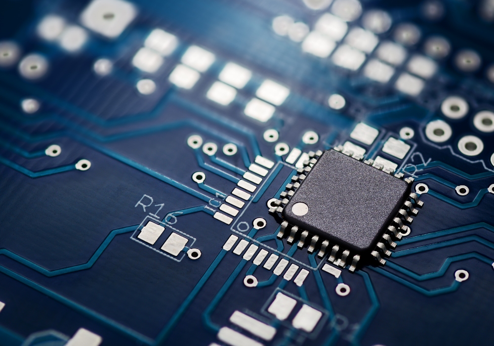
Printed circuit boards are used in electronic devices to provide a platform for mounting and interconnecting various electronic components. At PCB board level, PCB shielding typically comes in the form of metallic enclosures or cans designed to surround and protect sensitive circuitry. These enclosures are made of materials with high electrical conductivity. The shielding acts as a physical barrier that blocks or redirects electromagnetic waves, reducing the impact of EMI and radio frequency interference (RFI).
Why is PCB Shielding Important?
PCB shielding plays a pivotal role in upholding the integrity and functionality of electronic devices, especially as electronic components become more sensitive to electromagnetic interference.
From smartphones to critical medical devices, EMI has the potential to disrupt their operation, leading to malfunctions. Ensuring effective shielding is paramount in mitigating potential risks, safeguarding against disruptions in signal transmission and performance degradation.
Applications of PCB Shielding
The applications of PCB shielding are vast and critical across various industries:
- Consumer Electronics: Ensures optimal performance in smartphones and laptops.
- Medical Equipment: Vital for accurate readings and patient safety in MRI machines and pacemakers.
- Automotive Electronics: Maintains reliable operation in control units and infotainment systems.
- Telecommunications: Essential for uninterrupted communication in infrastructure.
- Aerospace and Defence: Ensures reliability in avionics and defence systems.
- Industrial Automation and Energy Systems: Prevents interference in critical industrial applications.
To summarise, EMI and RFI shielding remains fundamental for preserving data integrity, ensuring device reliability and promoting safety.
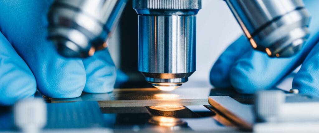
What are the Materials Used in PCB Shielding?
When choosing metals for EMI and RFI shielding at PCB board level, engineers must consider factors such as electrical conductivity, thermal stability, mechanical properties, shielding effectiveness and cost.
Copper, Brass, Beryllium Copper and Phosphor Bronze
Copper and its alloys are used for PCB shielding due to its high electrical conductivity, enabling it to efficiently conduct electromagnetic waves, minimising EMI and offering flexibility in design shielding solutions. However, copper is prone to oxidation, which can reduce its shielding performance over time, resulting in tin plating for enhanced longevity and solderability.
Nickel silver
Nickel silver exhibits high electrical conductivity, reducing electromagnetic interference. Nickel silver is also known for its corrosion resistance, which ensures long-term performance and durability in harsh environments. Furthermore, it has excellent strength, can be soldered and has effective magnetic permeability.
Tin-plated mild steel
Tin-plated mild steel serves as a material for shielding cans due to its strength and permeability, coupled with its cost-effectiveness compared to alternative metals. While steel may not match the electrical conductivity of beryllium copper, the tin plating on steel serves a dual purpose. It provides corrosion protection, preventing rust, and offers a favourable solderable surface for attaching the shield to the traces on the surface board during assembly.
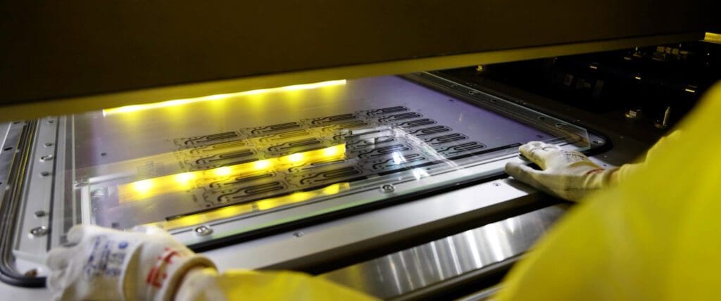
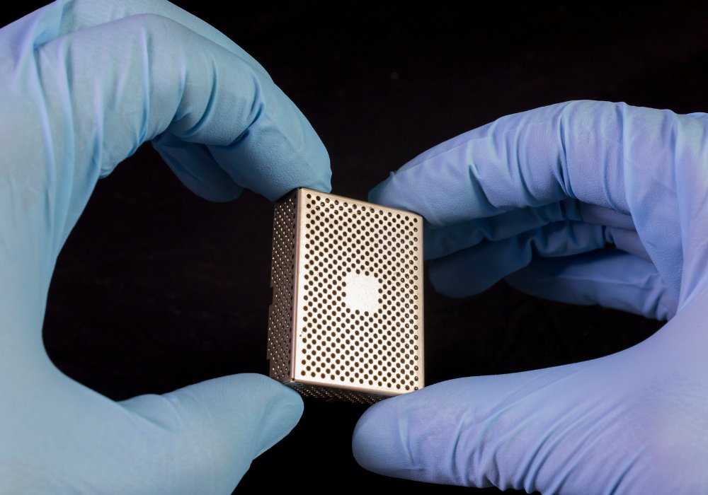
Manufacturing Processes Used to Produce PCB Shielding
Two common manufacturing processes for producing PCB shielding cans are stamping and photochemical etching.
Stamping PCB shielding
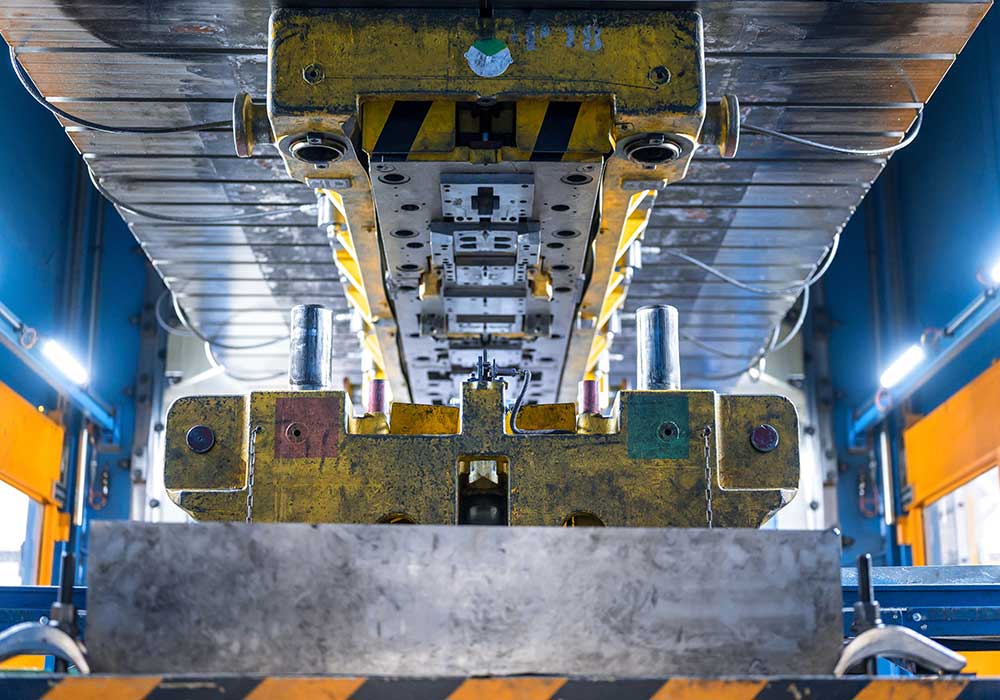
Stamping involves using a die to cut or shape a flat sheet of metal into the desired part specifications. While advantageous for repeatability and efficiency in high-volume production, stamping has drawbacks such as increased tooling costs and prolonged lead times, especially for custom designs and lower production runs.
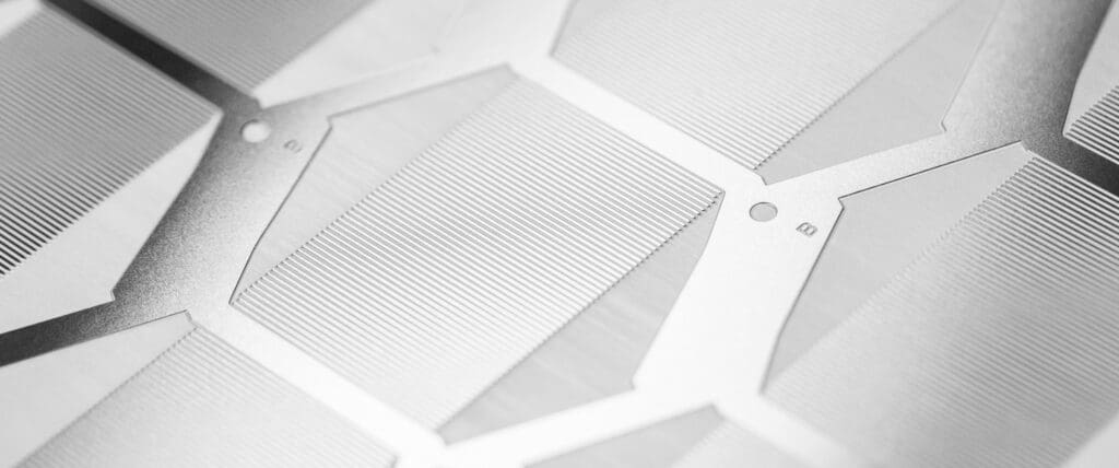
Photochemical etching PCB shielding
Chemical etching, a subtractive manufacturing process utilising chemical etchants to selectively remove material from a metal sheet, offers numerous advantages in PCB shielding can production. Compared to stamping, photochemical etching is highly versatile. Digital tooling eliminates the need for expensive hard tooling, reducing production lead times and costs while enabling intricate designs and value-added features such as ventilation, access holes, fold lines for hand forming, part numbers and logos, without incurring additional costs.
Conclusion
In the ever-advancing landscape of technology, effective PCB shielding is crucial to manage EMI risks, ensuring the sustained reliability and optimal performance of electronic devices across various industries. Engineers must carefully navigate material selection intricacies, striking a balance between conductivity and durability when designing board-level shielding solutions. Chemical etching emerges as a standout manufacturing option for flexibility, speed and cost-effectiveness—particularly beneficial for intricate or custom designs in our dynamic technological era. Conversely, stamping proves advantageous for high-volume production, offering repeatability and efficiency when high upfront tooling costs can be justified.
Chemical Etching Whitepaper
Learn how chemical etching can overcome the limitations of traditional sheet metal machining technologies.
DownloadLatest Articles